Nvidia said it had no need for the NAND memory standard, and Google just joined the alliance behind it
NVIDIA still does not appear interested in HBF. Its view is that HBF's high bandwidth can be sufficiently addressed with eSSDs.
Google currently appears to be the most aggressive player pushing HBF.
Google has put its name on the HBF standards alliance led by SK hynix and SanDisk. On the same day, the alliance published its first technical specification.
 SanDisk and SK hynix release the first OCP technical specification for High Bandwidth Flash (SanDisk press release, 2026-08-03)
The release names four contributors: SanDisk, SK hynix, Google and Tenstorrent. Tenstorrent designs its own AI accelerator chips. Nvidia is not on the list.
Why put NAND next to a GPU

NAND is the chip that holds the photos on your phone and the files on your laptop. It keeps data without power, and in exchange it is slower than DRAM. That is why NAND has lived in the storage slot rather than beside the GPU. The seat next to the GPU only had to be fast, and HBM, which is DRAM stacked in layers, was sitting in it. HBF proposes stacking NAND in that same seat instead. It is slower, and it holds far more. The premise is that what runs short when you serve an AI model is not only speed but somewhere to put things.

What the specification stakes out
The author reports only that Google has joined. Open the specification and you can see where this part means to sit. What it holds is a multiple of what a single HBM stack carries, while the bandwidth written into the spec is quoted in different units altogether from the terabytes per second HBM advertises. This is not a part that pushes HBM aside on speed. It is a part that takes on capacity.
Retrieved 2026-08-04 · OCP High Bandwidth Flash first technical specification, announced by SanDisk and SK hynix on 2026-08-03 · figures as reported by The Korea Times, 2026-08-04
 SK hynix and SanDisk unveil standards for high-bandwidth flash memory (The Korea Times, 2026-08-04)
The Korea Times reports that the specification uses UCIe as the road connecting HBF to the processor. UCIe is a shared standard for linking chip pieces made by different companies inside one package. That choice says what kind of part this is meant to be. Not a component fitted to one accelerator maker's design, but one that anyone can bolt onto the side of their own chip.
The seat Nvidia left empty
If more bandwidth is needed, enterprise SSDs are enough. There is no reason to bring a new standard inside the package.
As inference grows, what runs short is room, not speed. An SSD sits outside the package, and that distance costs time.
Faced with the same need, one side sees it solved by parts that already exist, the other sees a seat that has to be built.
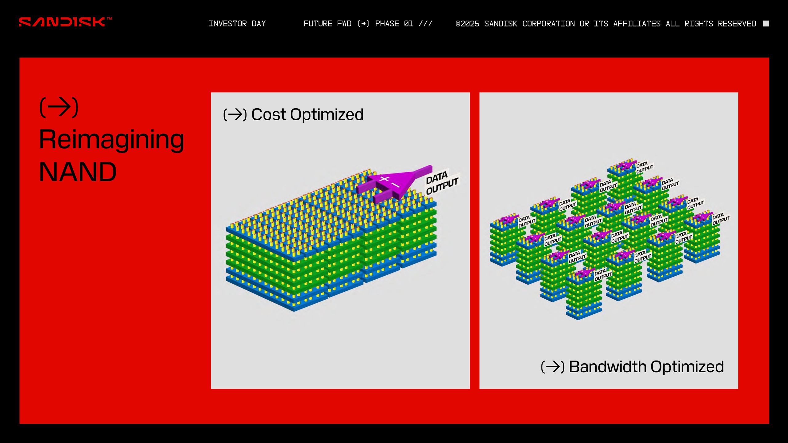 SanDisk and SK hynix join forces to standardize High Bandwidth Flash, a NAND-based alternative to HBM, at 8-16x the capacity of DRAM (Tom's Hardware, 2025-08-07)
When the alliance first formed in August 2025, Tom's Hardware reported that HBF was aiming to hold 8 to 16 times what HBM holds at comparable cost. If the cost is the same and the room is several times larger, the company with the strongest reason to push this standard is the one that keeps its own models parked in its own data centres and runs them all day. That is the seat Google walked into first.
Google and Tenstorrent step forward in 2026
The alliance was formed in February 2026 and produced its first specification six months later. For standards work, that is unusually quick. The author writes that SK hynix is more proactive on HBF than Samsung. Even so, he expects both to show samples and begin customer qualification in the second half of this year. The empty seat where Nvidia would be is both this standard's weakness and its reason for existing. If the company holding most of the accelerator market does not use it, volume never arrives. At the same time, carving out one memory slot that company does not get to define is exactly why Google and Tenstorrent walked in. Whether the document turns into a product shows up in the samples and the qualification runs this half.
- Google and Tenstorrent are named as contributors to a standard that stacks NAND, not DRAM, beside the GPU, and the first specification landed the same day.
- With a standard in place, SK hynix and SanDisk can sell NAND at the price of a seat next to the GPU rather than at storage prices.
- How much of that seat actually gets filled now depends on how much Google and Tenstorrent buy, with Nvidia absent.
Scheduled for gradingAwaiting grading
Sources
- Original Jukan (@jukan05) · Google has joined the HBF consortium · 2026-08-04
- SanDisk press release SanDisk and SK hynix release the first OCP technical specification for High Bandwidth Flash, with Google and Tenstorrent as contributors (2026-08-03)
- The Korea Times HBF specification figures: 8-high and 16-high stacks up to 512GB, 0.4-3.0Tbps, connected over UCIe (2026-08-04)
- Tom's Hardware Report at the time the alliance formed: HBF targets 8-16x the capacity of HBM at comparable cost (2025-08-07)
Retrieved 2026-08-04 · Specification figures follow the first OCP technical specification released 2026-08-03; sample and qualification timing is the author's and the companies' expectation.
This author's record
- BullNvidia looks set to halve the HBM going into Rubin Ultra, and it is not because…
- BullThree years of Samsung's profit buys Samsung and leaves 131 trillion won
- BullWhy does Samsung collect the full price increase on a five-year contract when M…